Infrared Heart Rate Monitor
A photoplethysmography pulse sensor built from scratch with IR LED, photodiode, and analog signal conditioning, for a Biophotonics module project
A module project for the Biophotonics course, Biomedical Engineering School, International University, Vietnam National University HCMC.
In theory, this was a project about light-tissue interaction, the Beer-Lambert Law, and the optical properties of blood. In practice, it was mostly about why the circuit kept producing noise that looked suspiciously more like a guitar amplifier than a heartbeat. We learned a lot of biophotonics. We also learned what a bad solder joint sounds like on an oscilloscope.
The Physics (The Part We Were Supposed to Focus On)
Photoplethysmography is an optical technique that detects volumetric changes in blood circulation through a tissue bed. The principle is straightforward: shine infrared light through a fingertip, and measure how much comes out the other side.
Blood absorbs infrared light. Oxygenated hemoglobin (HbO₂) and deoxygenated hemoglobin (Hb) have distinct absorption spectra, which is the basis of pulse oximetry (SpO₂). For a simple heart rate monitor, we care only about total absorption, not the ratio between the two species, so a single IR wavelength suffices.
As the heart beats, arterial blood pressure rises and the arterioles in the fingertip dilate slightly. This briefly increases the optical path length through blood, raising absorption and reducing the transmitted intensity reaching the photodiode. The result is a small periodic modulation riding on top of a large DC signal: the DC component corresponds to steady absorption by tissue, venous blood, and average arterial blood; the AC component (the PPG waveform) corresponds to pulsatile arterial flow and occurs at the heart rate frequency, typically 0.5 to 3 Hz.
The amplitude of this AC component is tiny. Typical modulation depth is 0.5 to 2% of the DC level, which means the signal of interest is roughly two orders of magnitude smaller than the background it sits on. That ratio is why the signal conditioning circuit is not optional.
System Overview
The full system has four layers:
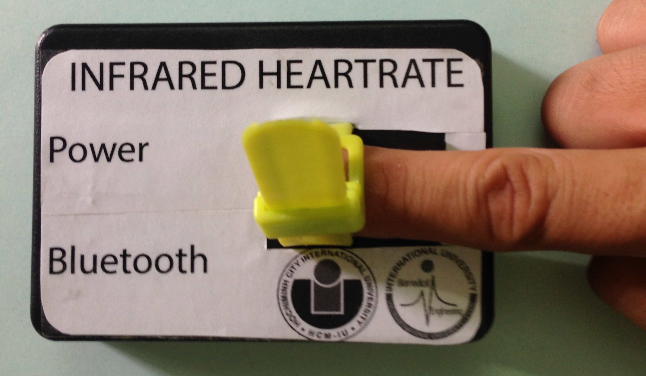
- Optical sensor — a transmissive finger clip with an 940 nm IR LED on one side and a photodiode on the other
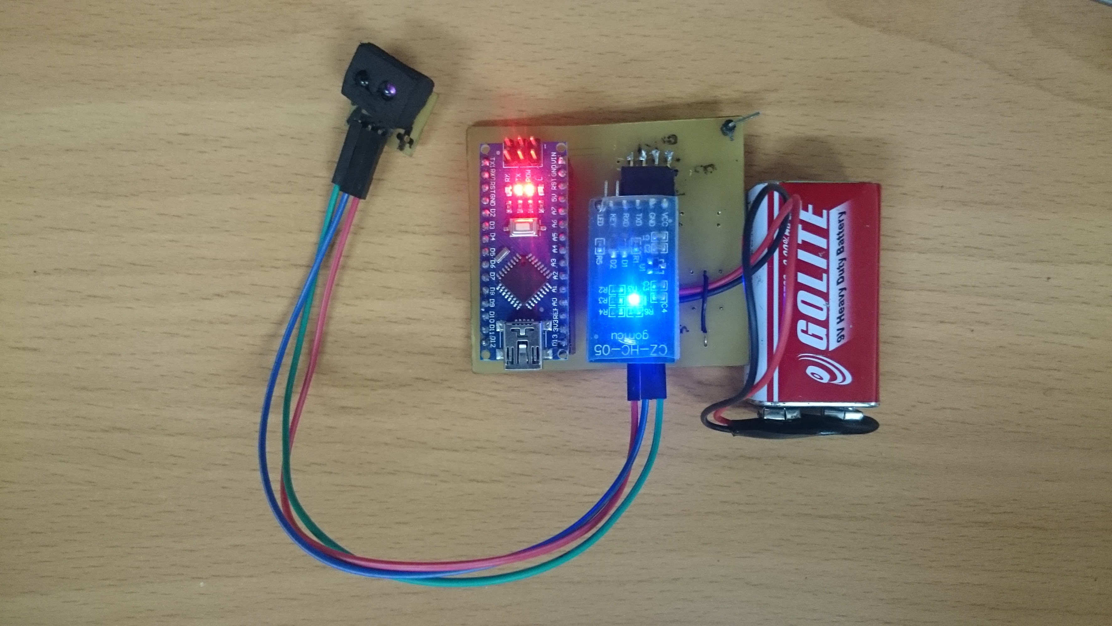
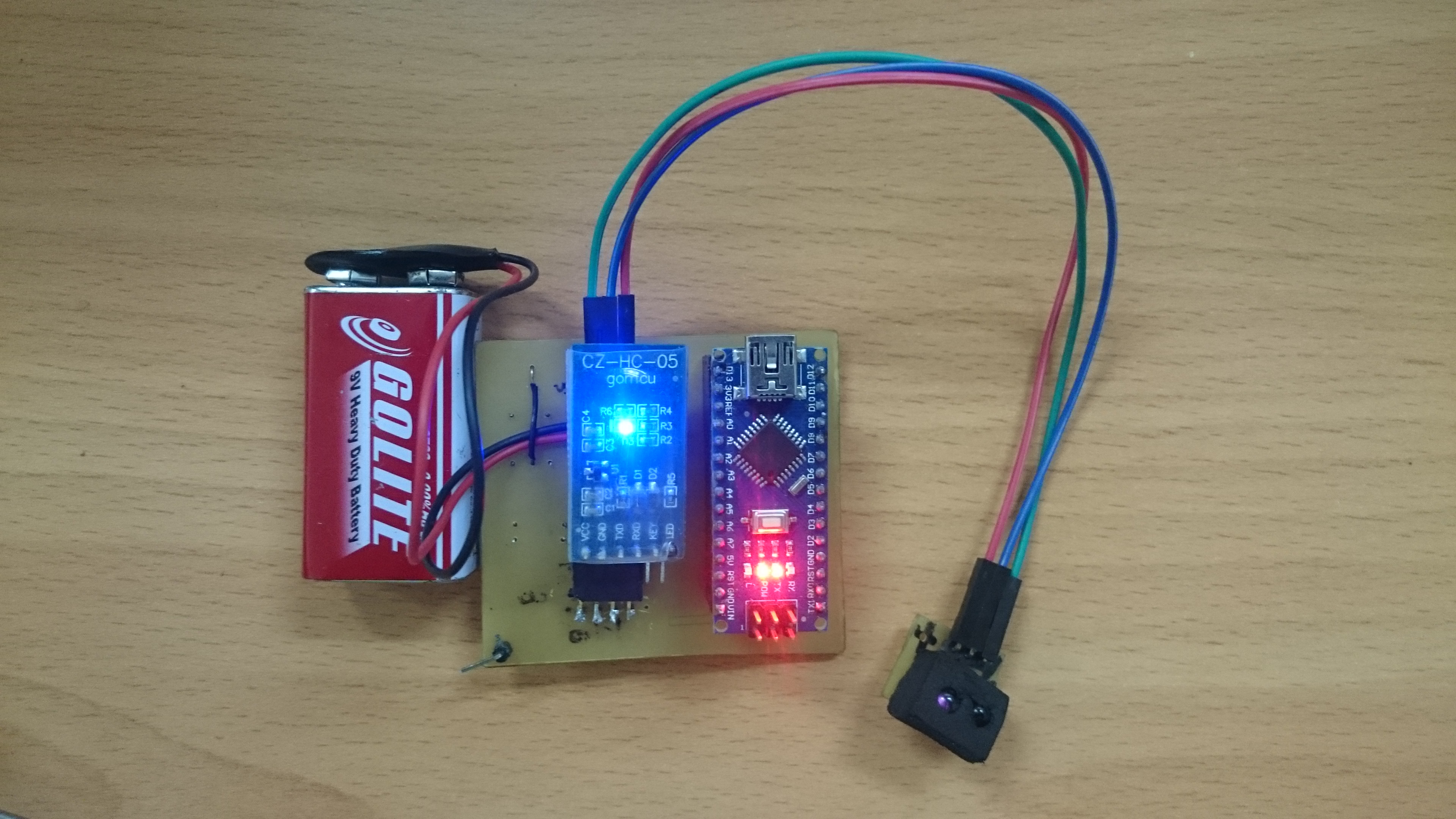
- Analog signal conditioning PCB — four stages built around TL082 and LM324 op-amps, powered by a 9V battery
- Microcontroller and wireless link — Arduino Nano digitising the conditioned signal, HC-05 Bluetooth module transmitting to a host
- Software — a MATLAB GUI for real-time display and heart rate computation, with a companion Android app for wireless readout
Circuit Design
The schematic below shows the four stages of the analog front-end. This is where most of the project time was spent, and also where most of the suffering happened.
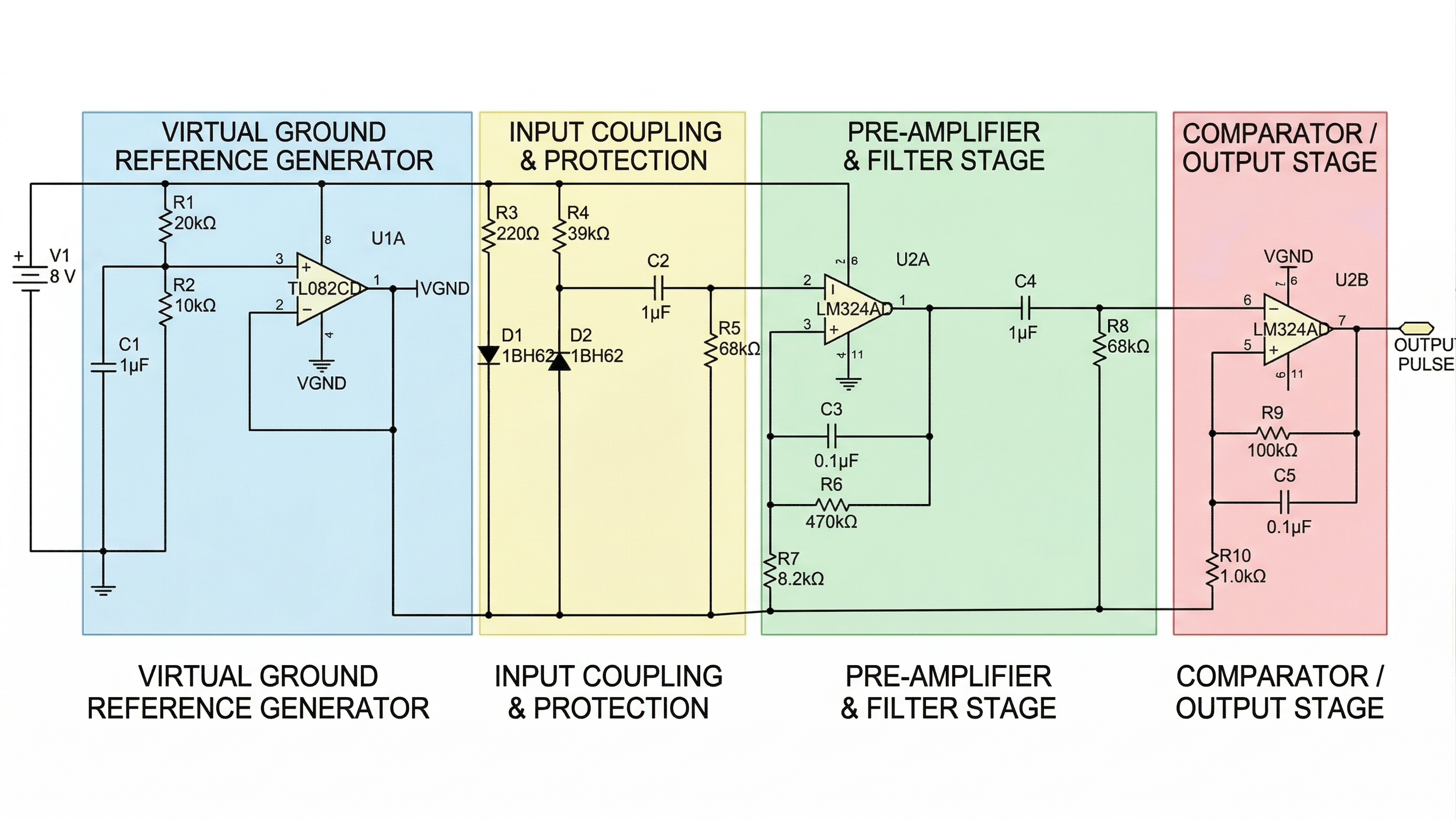
Stage 1: Virtual Ground Reference Generator
The entire circuit runs off a single 9V battery, but op-amps designed for bipolar AC signals need a reference point somewhere between the supply rails to handle both positive and negative signal excursions. Rather than using a split supply (two batteries), we created a virtual ground at half the supply voltage (~4.5V) using the TL082 (U1A) in a voltage follower configuration, driven by a resistor divider (R1 = 20 kΩ, R2 = 10 kΩ) and buffered with a bypass capacitor (C1 = 1 µF).
The output of this stage, labelled VGND throughout the schematic, is the signal reference for all subsequent stages. Getting this stable mattered a great deal: any ripple on VGND appeared as common-mode noise amplified through every stage downstream.
Stage 2: Input Coupling and Protection
The raw photodiode output carries a large DC offset (steady ambient and LED light) with a small AC PPG signal on top. This stage uses a series capacitor (C2 = 1 µF) to AC-couple the signal, blocking the DC and passing only the heartbeat-frequency AC component. Resistors R3 (220 Ω) and R4 (10 kΩ) set the high-pass cutoff and provide a discharge path for the capacitor. Two Schottky diodes (D1 and D2, 1BH62) clamp the input against voltage spikes that could damage the downstream op-amps, particularly if the LED drive current is adjusted or fingers are swapped in and out rapidly.
This stage is deceptively important. Without proper AC coupling, the DC offset from the photodiode would saturate the amplifiers before any gain was applied to the actual signal.
Stage 3: Pre-Amplifier and Filter Stage
This is the heart of the signal chain, and the stage that caused the most grief. The LM324 (U2A) is configured as an inverting bandpass amplifier that does two things simultaneously: amplifies the PPG signal to a useful voltage range, and rejects frequencies outside the physiological heart rate band.
The component values set the frequency response:
- High-pass pole (R5 = 68 kΩ, C2 = 1 µF): cutoff around 0.5 Hz, blocking residual DC drift from the coupling stage and very slow baseline wander
- Low-pass pole (R6 = 470 kΩ, C3 = 0.1 µF, C4 = 1 µF): cutoff around 3 Hz, attenuating high-frequency noise and 50 Hz mains interference
- Gain (R6 / R5 = 470 kΩ / 68 kΩ ≈ 6.9 in the passband), further boosted by R7 (4.2 kΩ) in the feedback network
The targeted pass-band of roughly 0.5 to 3 Hz corresponds to 30 to 180 BPM, covering the full physiological heart rate range. In principle, this is clean and elegant. In practice, the gain was high enough that any 50 Hz pickup on the breadboard traces appeared as a loud hum on the oscilloscope that completely buried the 1 Hz PPG signal. The fix involved shortening every wire, twisting the LED and photodiode leads together, and adding the bypass capacitors that had been optimistically omitted from the first build.
Stage 4: Comparator and Output Stage
The amplified PPG waveform from Stage 3 is still an analog signal. The comparator stage (LM324 U2B) converts it into a clean digital pulse by comparing it against the VGND reference. When the signal crosses the threshold on each heartbeat, the output swings to the supply rail, producing a square pulse. R8 (68 kΩ) and R9 (100 kΩ) set the hysteresis on the comparator to prevent multiple triggering on a noisy zero-crossing. R10 (1.0 kΩ) and C5 (0.1 µF) on the output provide a small RC filter to debounce the edge.
This pulse output can be fed directly to a microcontroller interrupt pin and timed to compute beats per minute without any further signal processing, which is exactly how the Arduino firmware worked.
The PCB
After iterating on a breadboard until the signal was clean enough to be recognisable as a heartbeat (rather than, say, a damaged fan), the circuit was transferred to a custom etched PCB.
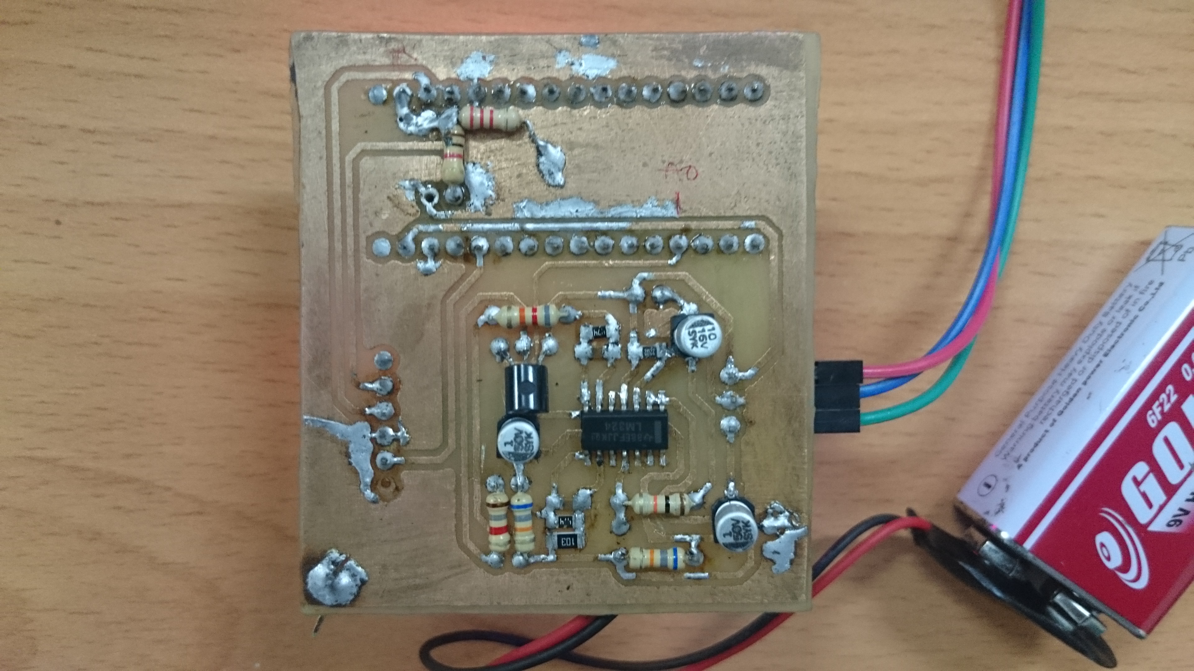
The board integrates the analog conditioning circuit, Arduino Nano (for ADC and Bluetooth), and HC-05 module, all powered from the 9V battery through a simple linear regulator. The finger clip sensor connects via a short cable and a header, which proved important because earlier builds with a fixed cable meant that every time a new finger was tried, the entire assembly needed to be repositioned.
Firmware and Software
The Arduino firmware was minimal by design: read the ADC at 100 Hz, detect rising edges on the pulse output from Stage 4, timestamp them, and stream the raw ADC values and inter-beat intervals over Bluetooth to the host.
The MATLAB GUI handled the heavier processing: real-time plotting of the raw PPG waveform, peak detection on a rolling window, BPM calculation from the average of the last five inter-beat intervals, and a basic quality indicator that flagged readings with high variance as motion artifact.
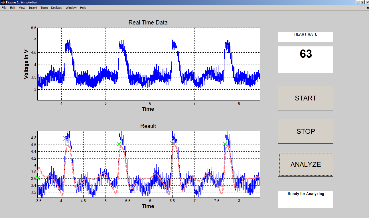
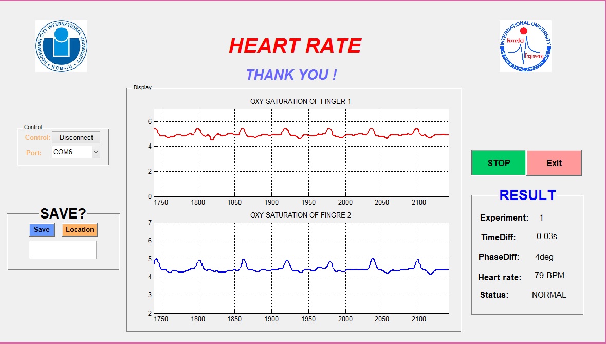
A second MATLAB view showed the results of a two-channel measurement used to compute the phase difference between PPG signals at two finger positions, a concept from the course that relates to pulse wave velocity and arterial stiffness.
The Android app provided a wireless readout of the live BPM over Bluetooth, without needing a laptop nearby.
What Actually Took the Most Time
The biophotonics was genuinely interesting. The Beer-Lambert Law, absorption spectra of hemoglobin, the difference between transmissive and reflective PPG modes, how SpO₂ oximetry exploits the isosbestic point of Hb and HbO₂ at 805 nm. All of that took maybe 20% of the project time.
The other 80% was approximately this:
- Getting the virtual ground stable. Any load on VGND caused it to droop, which shifted the operating point of every stage simultaneously. The fix was adding more bypass capacitance than seemed reasonable.
- 50 Hz mains pickup. The gain in Stage 3 was high enough that even the wiring on the bench acted as an antenna. Solved by shortening leads, twisting the sensor cable, and accepting that some days the noise floor was just higher than others.
- Comparator chatter. The first version of Stage 4 had no hysteresis, so a noisy PPG peak triggered the comparator four or five times instead of once. This produced heart rates in the range of 400 BPM, which is alarming. R9 and the hysteresis network fixed it.
- Motion artifact. Any slight movement of the finger produced an artifact ten times the amplitude of the actual heartbeat. The solution was to ask subjects to hold very still and to breathe shallowly. Not a clinical-grade solution.
- The solder joint on R7. It looked fine. It was not fine. It took two days to find.
Conclusion
The device worked. Not on the first build, not on the second, but eventually it produced a clean 1 Hz waveform from a fingertip, turned it into a BPM readout, and transmitted it wirelessly to a screen. That felt like a genuine achievement at the time, and honestly still does.
The deeper lesson, which the course did not explicitly teach but definitely delivered, is that a well-understood signal chain on paper can be humbled by a loose wire. Biophotonics explains why the signal exists. Analog circuit engineering explains whether you can actually measure it. The two skills do not automatically come together, and the gap between them is where most of the real work lives.